
TECHNOLOGY
The company has rich management and operation experience, strong technical force, advanced production technology,
sophisticated production equipment, complete testing methods, reliable product quality, and thoughtful after-sales service.
New trends in the development of power semiconductor modules
- Categories:Technical Support
- Author:
- Origin:
- Time of issue:2013-05-27
- Views:0
(Summary description)However, with the increase of module frequency and power, the general IGBT module structure with large internal parasitic inductance can no longer meet the needs of applications. In order to reduce the assembly parasitic inductance inside the module and minimize the overvoltage generated by the device during switching to meet the needs of FM high-power IGBT module packaging, ABB has developed a planar low-inductance module (ELIP) as shown in Figure 3. ). The main difference between this structure and the general traditional structure is: (1) It uses a lot of wide and thin copper sheets to overlap to form the emitter terminal and the collector terminal. When installed, it is parallel to the module copper base plate and is of equal length. The parallel wires are directly connected from the IGBT emitter to the emitter terminal, and the collector terminal is connected to the DBC board space position, thereby eliminating mutual inductance, limiting the proximity effect, and reducing the internal parasitic inductance; (2) many parallel connections Both the IGBT and FWD chips are soldered on the DBC board without graphics, and the emitter of the IGBT and the anode of the FWD are soldered with molybdenum buffer sheets. The current distribution is consistent with the rectified voltage conditions, which is beneficial for the module chip to work at the same temperature, which greatly improves the output and reliability of the module; (3) The module adopts a stacked design, which combines upper and lower insulation layers, upper and lower electrode terminals and printed circuits The plates are stacked on each other and glued together (to avoid air bubbles when bonding), which can be cycled well with temperature, without considering the so-called welding stress, that is, the so-called "S"-shaped electrode design.
Since the IGBT of the MOS structure is voltage-driven, the driving power is small, and IC can be used to drive and control, and then developed to the IGBT chip, fast diode chip, control and drive circuit, overvoltage, overcurrent, overheating and undervoltage The intelligent IGBT module (IPM), which is packaged in the same insulating housing such as protection circuit, clamping circuit and self-diagnostic circuit, creates devices for high frequency, miniaturization, high reliability and high performance of power electronic inverters The foundation also simplifies the design of the complete machine, reduces the design, development and manufacturing costs of the complete machine, and shortens the time to market for the complete machine product. Because the IPM adopts a standardized grid control interface with logic level, the IPM can be easily connected to the control circuit board. The self-protection ability of IPM in the event of a fault reduces the damage of the device during development and use, and greatly improves the reliability of the whole machine.
New trends in the development of power semiconductor modules
(Summary description)However, with the increase of module frequency and power, the general IGBT module structure with large internal parasitic inductance can no longer meet the needs of applications. In order to reduce the assembly parasitic inductance inside the module and minimize the overvoltage generated by the device during switching to meet the needs of FM high-power IGBT module packaging, ABB has developed a planar low-inductance module (ELIP) as shown in Figure 3. ). The main difference between this structure and the general traditional structure is: (1) It uses a lot of wide and thin copper sheets to overlap to form the emitter terminal and the collector terminal. When installed, it is parallel to the module copper base plate and is of equal length. The parallel wires are directly connected from the IGBT emitter to the emitter terminal, and the collector terminal is connected to the DBC board space position, thereby eliminating mutual inductance, limiting the proximity effect, and reducing the internal parasitic inductance; (2) many parallel connections Both the IGBT and FWD chips are soldered on the DBC board without graphics, and the emitter of the IGBT and the anode of the FWD are soldered with molybdenum buffer sheets. The current distribution is consistent with the rectified voltage conditions, which is beneficial for the module chip to work at the same temperature, which greatly improves the output and reliability of the module; (3) The module adopts a stacked design, which combines upper and lower insulation layers, upper and lower electrode terminals and printed circuits The plates are stacked on each other and glued together (to avoid air bubbles when bonding), which can be cycled well with temperature, without considering the so-called welding stress, that is, the so-called "S"-shaped electrode design.
Since the IGBT of the MOS structure is voltage-driven, the driving power is small, and IC can be used to drive and control, and then developed to the IGBT chip, fast diode chip, control and drive circuit, overvoltage, overcurrent, overheating and undervoltage The intelligent IGBT module (IPM), which is packaged in the same insulating housing such as protection circuit, clamping circuit and self-diagnostic circuit, creates devices for high frequency, miniaturization, high reliability and high performance of power electronic inverters The foundation also simplifies the design of the complete machine, reduces the design, development and manufacturing costs of the complete machine, and shortens the time to market for the complete machine product. Because the IPM adopts a standardized grid control interface with logic level, the IPM can be easily connected to the control circuit board. The self-protection ability of IPM in the event of a fault reduces the damage of the device during development and use, and greatly improves the reliability of the whole machine.
- Categories:Technical Support
- Author:
- Origin:
- Time of issue:2013-05-27
- Views:0
The birth of a new type of device often makes a huge change in the appearance of the entire device system and promotes the development of power electronics technology. Since the first thyristor came out in 1957, after more than 40 years of development and research, more than 40 kinds of power semiconductor devices such as turn-off thyristors (GTO) and insulated gate bipolar transistors (IGBT) have been introduced. The development trend of modularization, high-power, intelligence and modularization, this article will briefly introduce the development trend of modularization.
The so-called module was originally defined as connecting two or more power semiconductor chips according to a certain circuit, using protective materials such as RTV, elastic silicone gel, epoxy resin, etc., sealed in an insulating shell, and connected with a thermally conductive bottom plate. Insulated. Since Semikron Nurmbeg introduced the module principle (then only limited to thyristors and rectifier diodes) into the field of power electronics technology in the 1970s, modularity has been valued by power semiconductor companies around the world, and various forms of internal electrical connections have been developed and produced Power semiconductor modules, such as thyristors, rectifier diodes, bidirectional thyristors, reverse conducting thyristors, light-controlled thyristors, turn-off thyristors, power transistors (GTR), MOS controllable thyristors (MCT), power MOSFETs and insulated gate bipolar transistors ( IGBT) and other modules have enabled the rapid development of module technology, which accounts for an increasing proportion of devices.
According to statistics from the United States in the early 1990s, in the past ten years, the market share of discrete thyristors, rectifier diodes, and Darlington transistors of less than 300A, and Darlington transistors of more than 20A, has dropped from 90% to 20%. 10% rose to 80%, showing the rapid development of modules.
With the successful development of modern semiconductor devices based on MOS structure, that is, IGBTs, power MOSFETs, MOS-controlled thyristors (MCT) and MOC-controlled rectifiers (MCD) with voltage control, low drive power and simple control appeared, and developed An intelligent power semiconductor module, namely IPM, which combines device chips with control circuits, drive circuits, overvoltage, overcurrent, overheat and undervoltage protection circuits, and self-diagnostic circuits, and sealed in the same insulating housing.
In order to further improve the reliability of the system and adapt to the development direction of power electronics technology towards high frequency, miniaturization and modularization, some manufacturers have added some inverter functions on the basis of IPM, and the inverter circuit (IC ) Is packaged in a module in the form of a chip to become a user-specific power module (ASPM), so that it is no longer connected by traditional leads, and the internal wiring is connected by ultrasonic welding, thermal compression welding or crimping, so that The parasitic inductance is minimized, which is conducive to the high frequency of the device. A 7.5KW motor frequency conversion device, of which ASPM is only as large as 600×400×250 (mm), and the good news is that this kind of user-specific power module can be redesigned according to the application circuit, which has a great Application flexibility. However, it is technically difficult to integrate an integrated circuit IC with a logic level of a few volts and a few milliamps and a power semiconductor device with a few hundred amperes and a few thousand volts on the same chip. Although ASPMs below 1.5KW are currently on sale, a series of problems need to be solved to make high-power ASPMs. Therefore, people are forced to use hybrid packaging to manufacture integrated power electronic modules (IPEM) suitable for various occasions. IPEM has opened a new way for the development of power electronic technology in the new century.
Intelligent Thyristor Module
Thyristor and rectifier diode modules mainly refer to various electrically connected bridge arm modules and single-phase rectifier bridge modules. After nearly 30 years of development and production of thyristor modules, the technology for manufacturing this series of modules is quite mature and the production yield rate is also quite High, it is also very common and mature, and it has become an important device for power regulation, so it will not be introduced here.
The thyristor intelligent module is the ITPM (Intelligent thyristor power module), which is made by enclosing the main circuit of the thyristor, the phase-shifting trigger system, and the overcurrent and overvoltage protection sensors in a plastic shell. Because the thyristor is a current-controlled power semiconductor device, it needs a larger pulse trigger power to drive the thyristor, and some other auxiliary circuit components, such as a synchronous transformer for synchronizing current, are bulky. It is difficult to make the phase shift trigger system and The main circuit of the thyristor and the sensor are packaged in the same shell to make a thyristor intelligent module. Therefore, the world has never gotten rid of the traditional form of making thyristor devices and gate trigger systems separately.
Shandong Zibo Linzi Yinhe High-Tech Development Co., Ltd., after years of development and research, solved the problem of miniaturization of synchronous components and made them suitable for integrated applications, and then solved the problems of improving signal amplitude, anti-interference, high-voltage isolation, and synchronous signal input. , And developed high-density power pulse transformers and multiple high-speed high-current ICs, as well as two special ICs suitable for integrated modules. After using special materials such as DCB boards with good thermal conductivity and insulation properties, molybdenum copper boards, and elastic silicone gel with good electrical insulation and protection properties and good thermal conductivity, a variety of thyristor smart modules with various functions have been developed, such as Three-phase, single-phase integrated phase-shift control thyristor intelligent AC switch module, three-phase, single-phase AC switch module with zero-crossing trigger circuit, etc.
Figure 1 is the internal wiring diagram (a) and other appearance photos (b) of the thyristor intelligent three-phase bridge module, as well as the thyristor intelligent motor control module, which solves the thyristor main circuit and phase shift trigger system and protection sampling that have not been realized. The problem that sensors are packaged together in a plastic case. Linzi Yinhe has developed modules with a maximum working line current of 1600A (RMS) and rated working voltages of 380V and 600V. They have been used in AC frequency conversion, AC and DC electrical drives, three-phase AC solid-state switches and constant voltage and constant current power supplies.
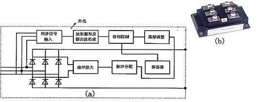
figure 1
IGBT smart module
In the early 1980s, the successful development of IGBT devices and the subsequent continuous improvement and improvement of their rated parameters played an important role in the development of high-frequency and higher-power applications. Because IGBT modules have voltage-based drives, they have low drive power. It has the advantages of high switching speed, reduced saturation voltage, high voltage and high current resistance, and excellent overall performance. It has become the most widely used power semiconductor device in the industrial field. Its hard switching frequency can reach 25KHz, and its soft switching frequency can reach 100KHz. The newly developed Thunderbolt IGBT has a hard switching frequency of 150KHz and a resonant inverter soft switching circuit of 300KHz.
At present, IGBT packaging forms mainly include plastic single tubes and modules in which the bottom plate and the main circuit are insulated from each other. High-power IGBT modules also have flat plate crimping forms. Since the closed form of the module is extremely convenient for designing radiators, it is widely adopted by major device companies. On the other hand, the production process of IGBT module is complicated. In the manufacturing process, a dozen or so fine lithography engravings are required, and the corresponding number of high-temperature processing is performed. Therefore, a large area, that is, a large current IGBT monolithic, will be manufactured. Greatly reduced. However, the MOS characteristics of IGBTs make it easier to connect in parallel, so the module package is more suitable for manufacturing high-current IGBTs. At first, because IGBTs used high-resistance epitaxial wafer technology, the voltage was difficult to break through, because to manufacture such high-voltage IGBTs, the epitaxial thickness must exceed micrometers, which is technically difficult and almost impossible to be practical.
In 1996, many Japanese companies used high-resistance silicon single crystals with a <110> crystal plane to manufacture IGBT devices. The thickness of the silicon wafer exceeded 300 microns, which made the single-chip IGBT withstand voltage exceeding 2.5KV. Therefore, in the same year, Toshiba launched the 1000A/2500V flat panel. The crimping type IGBT device is composed of 24 80A/2500V cores in parallel.
In 1998, ABB adopted a transparent P+ emitter layer and N-layer buffer layer structure on the anode side to make the IGBT module withstand voltage up to 4.5KV. The 1200A/3300V IGBT module developed by the company in the same year consisted of 20 IGBT chip and 12 FWD chips are made in parallel. Since then, the trial production of non-punch-through (NPT) and soft-punch-through (SPT) IGBTs has been successful, which makes IGBT devices have a positive temperature coefficient of resistance and is easier to connect in parallel. This makes high-voltage and high-current IGBT modules only need to be connected in parallel and not connected in series. technical foundation. At present, it has been able to mass-produce standard IGBT modules of 1, 2, 4, 6 and 7 units, and the highest level has reached 1800A/4500V. Figure 2 is a circuit diagram of a 300A/1700V IGBT module, which is composed of 4 160A/1700V IGBT chips and 8 100A/1700V fast recovery diodes.

figure 2
figure 1

Yinhe High-Tech Development
MESSAGE
- After-sales service
- Hotline +86-533-7216217
- Top
Copyright 2020 Zibo Linzi Yinhe High-Tech Development Co., Ltd. 鲁ICP备12000870号 Powered by www.300.cn